Coaxial Data Serialization & Power#
The major advantage of ONI-compliant headstages is that they contain onboard logic for controlling and streaming from arbitrary configurations of head-borne devices using a unified, bidirectional data stream. In this way, data can be sent to the PCIe Controller using modern serializer/deserializer (SERDES) chips that vastly reduce the amount of wiring required for communication between the headstage and the controller.
ONIX headstages use a coaxial serializer for communication. This chip provides power and bidirectional data transmission to and from from the headstage using a single coaxial cable (one signal wire and an outer shield). The coaxial cable is the only external connection to the headstage. Power (DC), a control “back-channel” (MHz), and a data “forward-channel” (GHz) occupy different portions of the RF spectrum and therefore can be resolved as distinct signal streams. Any high-quality 50-Ohm characteristic impedance cable with low loss in the GHz frequency range can be used to make this connection (e.g. SMA cables). However, the connection to the headstage is usually accomplished using specialized micro-coax cable that is extremely thin and flexible. We generally use cables that are 150-300 μm in diameter.
Note
Have a look at the Making Coaxial Tethers page for more details on micro-coax headstage tethers
ONIX headstages use an FPGA to control peripheral devices and combine their data streams prior to serialization. For instance, Headstage-64 and Neuropixels-1.0f Headstage use an Intel MAX10 FPGA. The exact FPGA is not important because every ONI-compliant headstage uses very similar gateware (gateware is FPGAs as firmware is to microcontrollers) that performs three major functions
Local Hardware Control Provides hardware controllers (SPI, I2C, etc), timing, and control logic for each of the sensors and actuators on the headstage
Data Streaming Provides a standard protocol for arbitrating access of each of the device data streams to the serializer.
Register Programming Provides a standard interface for bi-directional configuration and control of the devices on the headstage.
Power#
As mentioned in the previous section, power is DC-coupled into the coaxial link at the controller and recovered at the headstage via a second, inductive DC path. This “T-network” provides a low impedance path for the DC portion of the signal (power) and rejects the RF components so that they are preserved for communication between the SERDES pair.
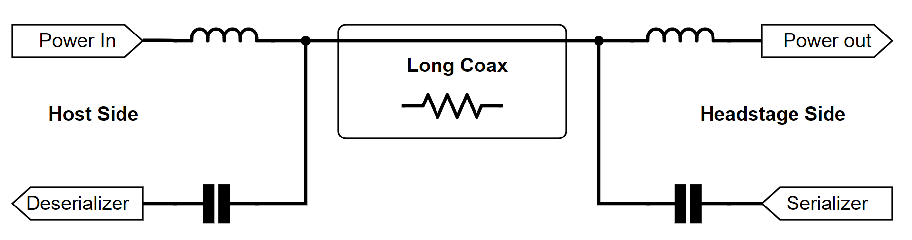
LC-network for combining power and data on the coaxial cable.#
Its important to note that this circuit is completely passive. Therefore whatever voltage is supplied at the controller side will end up at the input to the headstage. Care must be taken to make sure this voltage is appropriate.
Warning
Do not exceed the maximum voltage at the coaxial input to the headstage. Make sure you make this measurement at the headstage to account for a potential voltage drop in the tether. Exceeding this voltage can permanently damage some headstages (Headstage-64 in particular because it lacks an overvoltage lockout circuit)
Further, if a long and thin coaxial tether is used, the DC resistivity of the wire can accumulate, resulting in a significant voltage drop across the cable.
Note
Long, thin tethers can have a significant series resistance that results in a voltage drop across the length of the tether. This may have to be compensated for by tuning the controller input voltage to account for the drop. ONIX controllers have this ability (e.g. see PCIe Controller).
DS90UB933/4 Communication Protocols#
The DS90UB933/DS90UB934 are a coaxial SERDES pair used on several ONIX headstages and controller modules:
Headstage-64 (DS90UB933 Serializer)
Neuropixels-1.0f Headstage (DS90UB933 Serializer)
PCIe Controller (DS90UB934 Deserializer)
along with the UCLA Miniscope and its derivatives. This section describes how this SERDES pair is used for control of and communication with headstages.
Data Serialization#
The DS90UB933 is a 100 MHz parallel to coaxial serializer that is typically used for streaming camera data. ONIX headstages use an intermediate FPGA to translate data from any number of heterogeneous data sources to the serializer input using the following simple protocol
where the signal lines are defined as follows:
plck:The serializer’s pixel clock, repurposed for generic data transmission for ONIX headstages.
hsync:The horizontal synchronization signal, re-purposed on ONIX headstages to indicate the
databus contains a device ID on ONIX headstagesvsync:The vertical synchronization signal, re-purposed to indicate the
databus a CRC value for the preceeding packet on ONIX headstagesdata:The 12-bit data bus containing device ID, CRC value, or device data depending on the states of
hsyncandvsync
The ID is the device index within the device table, frame is a
device’s frame data, and CRC is a CRC-12 of the ID and
frame elements. See the ONI Specification for detailed descriptions of these
elements meaning.
These signal lines are present on the FPGA-side of both the serializer and deserializer, prior to headstage serialization and after deserialization, respectively. This means that the serializer link is effectively “invisible” from the controller’s perspective, and the headstage can be treated as if it was just a module connected to the controller itself.
During serialization, data are transmitted over the coaxial cable using an RF-encoding scheme called FDP Link III which embeds the clock in the data stream and allows for active equalization to compensate for imperfections in the cable. This link uses and 700 MHz carrier for high speed data and provides a low speed bidirectional link for sending triggers and configuration to the headstage.
Register Configuration#
The DS90UB933/DS90UB934 SERDES pair have a I2C-based backchannel for bidirectional communication. This channel is used for two purposes in ONIX hardware.
Device configuration via register writing and reading. e.g. setting and bandwidth of the filters on the Intan chip.
Flashing the headstage FPGA’s non-volatile memory with updated gateware.
The ONI Specification describes a register programming protocol that can be implemented using a 32-bit wishbone bus:
where the signal lines are defined as follows:
cyc:Transaction cycle / chip select
we:Write enable
addr:32-bit register address
wval:32-bit write value
ack:Acknowledge
err:Error
rval:32-bit read value
The cyc line is typically muxed to different devices in an acqustion
context using an auxilary 32-bit device index that is also required by the ONI
specification. This bus needs to be transmitted over the DS90UB933/4 I2C
backchannel to be used to configure headstage devices. We have developed a
simple Wishbone over I2C module to accomplish this. This module uses the
following 7-bit command words:
Value |
Diagram Code |
Description |
|---|---|---|
0x00 |
WE |
Write enable |
0x01 |
RR |
Read request |
0x02 |
R0 |
Read enable 0 |
0x03 |
R1 |
Read enable 1 |
0x04 |
R2 |
Read enable 2 |
0x05 |
W0 |
Read enable 3 |
0x06 |
W1 |
Read enable 4 |
0x07 |
S0 |
Status 0 |
0x08 |
S1 |
Status 1 |
0xFF |
NA |
Invalid |
along with a status register for reporting the validity of read and write operations:
An example write sequence on this bus is given below. The wishbone bus drives an I2C sequence that is interpreted on the headstage and used to recreate the wishbone signals locally.